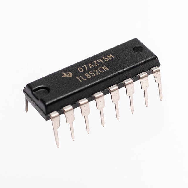
SensComp Electronic Component – TL852 Analog Integrated Circuit
Features
- Economical Ranging Control when used with TL851 Digital IC
- Operates With Single Supply Voltage.
- Digitally Controlled Variable-Gain Variable-Bandwidth Amplifier.
- Operational Frequency Range of 20 kHz to 90 kHz.
- Overall Gain Adjustment with One External Resistor.
- Interfaces to Electrostatic and Piezoelectric Transducers.
- TTL Compatible.
The TL852 Analog IC Chip is an economical sonar ranging receiver integrated circuit for use with the TL851 digital control integrated circuit. A minimum of external components is required for operation, and this amplifier easily interfaces to SensComp’s 50-kHz electrostatic transducers.
An external resistor from BIAS (pin 8) to GND (pin 16) provides the internal biasing reference. The amplifier’s gain can be set with a resistor from G1IN (pin 1) to GADJ (pin 3). Required amplifier gain will vary for different applications. A nominal peak-topeak value of 230 mV input during gain step 2 is recommended for most applications. For reliable operation, a level no lower than 50 mV should be used. The recommended detect level of 230 mV can be obtained for most amplifiers with an R1 value between 5000 ohm and 20,000 ohm. Digital control of amplifier gain is provided with gain control inputs GCA, GCB, GCC, and GCD. These inputs must be driven synchronously (all inputs stable within 0.1 ms) to avoid false receive output signals due to invalid logic counts. This can be done easily with the TL851 control integrated circuit. To dampen ringing of the 50-kHz electrostatic transducer, a 5000 ohm resistor from G1IN to XIN is recommended.
An external parallel combination of inductance and capacitance between LC and VCC provides an amplifier with an externally controlled gain and Q. This not only allows control of gain to compensate for attenuation of signal with distance, but also maximizes noise and sidelobe rejection. Care must be taken to accurately tune the LC combination at operating frequency or gain and Q will be greatly reduced at higher gain steps.
AC coupling between stages of the amplifier is accomplished with a 0.01 mf capacitor for proper biasing. The receive output is normally held at a low level by an internal 1 mA current source. When an input of sufficient amplitude is received, the output is driven alternately by the 1 mA discharge current and a 50 mA charging current. A 1000 pF capacitor is required from REC to GND to integrate the received signal so that one or two noise pulses will not be recognized.
XIN provides clamping for the transformer secondary when used for transducer transmit drive. The TL852 operates over a supply voltage of 4.5 volts to 6.8 volts (+5 volts DC nominal voltage) and is characterized for operation from -40°C to +85°C.

